New method of direct nanopore fabrication in tungsten oxide
News, 18 June 2025
An international research team from the Institute of Modern Physics of the Chinese Academy of Sciences (IMP CAS) and the Joint Institute for Nuclear Research studied the processes of tungsten oxide (WO3) nanostructuring. Using a combined experimental and numerical approach, the physicists presented a new method of directly forming nanopores in tungsten oxide using fast heavy ion irradiation. This method can be implemented in the creation of new materials with unique optical and electronic properties for photocatalysis and semiconductor electronics.
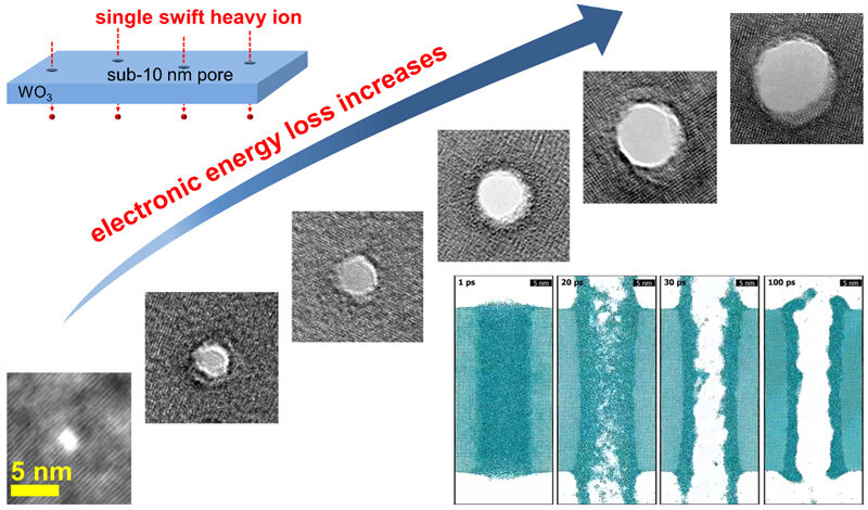 Formation of nanopores of less than 10 nm in WO3 films using fast heavy ion irradiation
Nanostructuring is the process of creating materials in which the size of structural elements is determined in the nanoscale range (up to hundreds of nanometers). Modern technologies for creating nanostructures allow controlling the shape, size, and spatial arrangement of nanoscale components. Thanks to this, nanostructured materials can have unique properties such as improved mechanical strength, electrical and thermal conductivity, optical properties, etc.
The formation of through nanopores in various materials is one of the most important aspects of nanostructuring. The most common method is focused ion or electron beam irradiation. A focused ion beam allows forming individual single pores while controlling their size and location. The pore fabrication rate is, however, low, which hinders the mass production of nanoporous materials. While being more effective, technologies based on electron beam irradiation are limited in terms of controlling the size and density of nanopores. Thus, it is crucial to introduce and develop novel approaches that will ensure the effective creation and tuning of nanopores.
Today, one of the promising methods for creating nanostructured materials is fast heavy ion irradiation. This technology is actively used to produce track membranes or “nuclear filters” with high selectivity, control critical parameters of high-temperature superconducting ceramics, create conductive pores in layered structures and form quantum dots.
At the Heavy Ion Research Facility (HIRFL) in Lanzhou (China), scientists irradiated WO3 films with argon, krypton, xenon, and tantalum ions with energies ranging from several hundred megaelectronvolts to several gigaelectronvolts using high energy heavy ion accelerators. During the experiments, it was found that irradiating tungsten oxide leads to the formation of through cylindrical nanopores with a thin amorphous shell.
By changing the ion energy, Chinese specialists were able to control the diameter of the resulting nanopores in the range from 1.8 to 7.4 nm with high accuracy. The creation efficiency of nanopores achieved almost 100% when tungsten oxide was irradiated with tungsten oxide. Sample critical thickness was calculated to be about 120 nm. The formation of through nanopores at this thickness is one of the key factors determining the possibility of producing nanomembranes using irradiation.
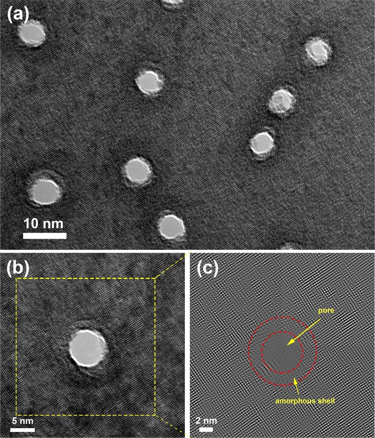 Pores formed by irradiation with 533 MeV Xe ions
“The Sector of Ion Implantation Nanotechnology and Radiation Materials Science of the Laboratory of Nuclear Reactions (FLNR) at JINR studying the radiation effects of fast ions in solids. While specialists from the Institute of Modern Physics of the Chinese Academy of Sciences are mainly engaged in creating new nanostructures in materials using irradiation, i.e. nanostructuring, I am interested in all tasks as somebody involved in modelling radiation effects,” a senior researcher at the FLNR JINR Sector of Ion Implantation Nanotechnology and Radiation Materials Science Ruslan Rymzhanov noted.
With the help of molecular dynamic modelling conducted by a scientist from the Joint Institute, the kinetics and mechanisms of nanopore formation in tungsten oxide were described as part of the study. As a result, the key parameters for the formation of through nanopores were calculated: viscosity (0.55 ± 0.01 MPa·s) and surface tension (91.5 ± 8.1 mN/m) of molten WO3. Based on a comparative analysis of these parameters with the properties of other materials, it is assumed that this value range contributes to a faster movement of the melt through the nanopore and its more abrupt release from the surface at the initial stages of the nanostructure formation, thus leading to the creation of through pores.
All computation was conducted using the Govorun Supercomputer based on the heterogeneous HybriLIT Platform of the Laboratory of Information Technologies at JINR, Kurchatov Institute‘s computing cluster, and the Lomonosov-2 Supercomputer cluster at the Research Computing Centre of Moscow State University.
Molecular dynamic modelling was carried out using an original multiscale approach developed by the international scientific team. In addition to the JINR specialists, it includes representatives of the Lebedev Physical Institute of the Russian Academy of Sciences (LPI RAS), the Kurchatov Institute, and the Institute of Plasma Physics of the Czech Academy of Sciences (IPP). As part of the team’s research, a new Monte Carlo model was developed, capable of describing the processes of interaction of fast heavy ions with solids. In particular, it provides insights into how exactly ionisation processes occur, how an excited electronic subsystem will evolve in the future, and how energy is transferred to an atomic subsystem. The results of calculations using the new model are used as initial data for the molecular dynamics method.
As the FLNR JINR researcher explained, the current interest among scientists in using ionising radiation for nanostructuring is quite reasonable. Irradiation with high energy heavy ions usually creates uniformly distributed nanopores of approximately the same size, which is an important factor for the development of filter materials and devices. In addition, for example, irradiation of layered nanostructures with heavy ions allows creating special nanoscale regions – quantum dots.
This article is just one stage in heavy ion physics research. Scientists have already studied the effects in massive samples, on the surfaces of materials, and in thin films of matter. The next stage of the scientists’ work will be the study of heavy ions’ effects in nanocomposites – complex materials consisting of several compounds. Other new research are planned to focus on layered nanostructures, which include semiconductors, metals, and other structures. The results of this work can be used to improve and modernise nanostructuring methods in electronic device production.