Graphene-based Planar Tunnel Electronics
News, 19 July 2021
First JINR Prize 2020 in the nomination “For theoretical Physics Research” was presented to the team of authors V. L. Katkov and V. A. Osipov from the Bogoliubov Laboratory of Theoretical Physics for their series of scientific papers “Graphene-based Planar Tunnel Electronics”.
“All technologies based on graphene are in the area of ideas or unique tested experimental developments (the transistor of Novoselov and others, 2013). There are none actual practical of graphene in the electronics, despite the fact that the Nobel Prize in physics was awarded “for graphene” in 2010. The silicon technology dominates at this moment, and graphene as silicon’s alternative is a long-term perspective. Basic research do not always reaches immediate practical success. For example, an ordinary field-effect transistor that is a basic part of all modern electronics, was patented in 1926, and was created after World War II, only in 1960. Our idea was patented but it has practical difficulties of creation the “nanogap”. However, it gave rise to other ideas in this direction, in particular, the “Valley Transistor” was proposed as an analog of our transistor (patent RU188856U1, Shelykh, Iorsh, ITMO, 2018). Time will show what will work in the end. Activities that at least slightly improve the perspective are a common task of scientists working at the forefront of science,” the authors of the scientific paper noted anticipating the story about their research.
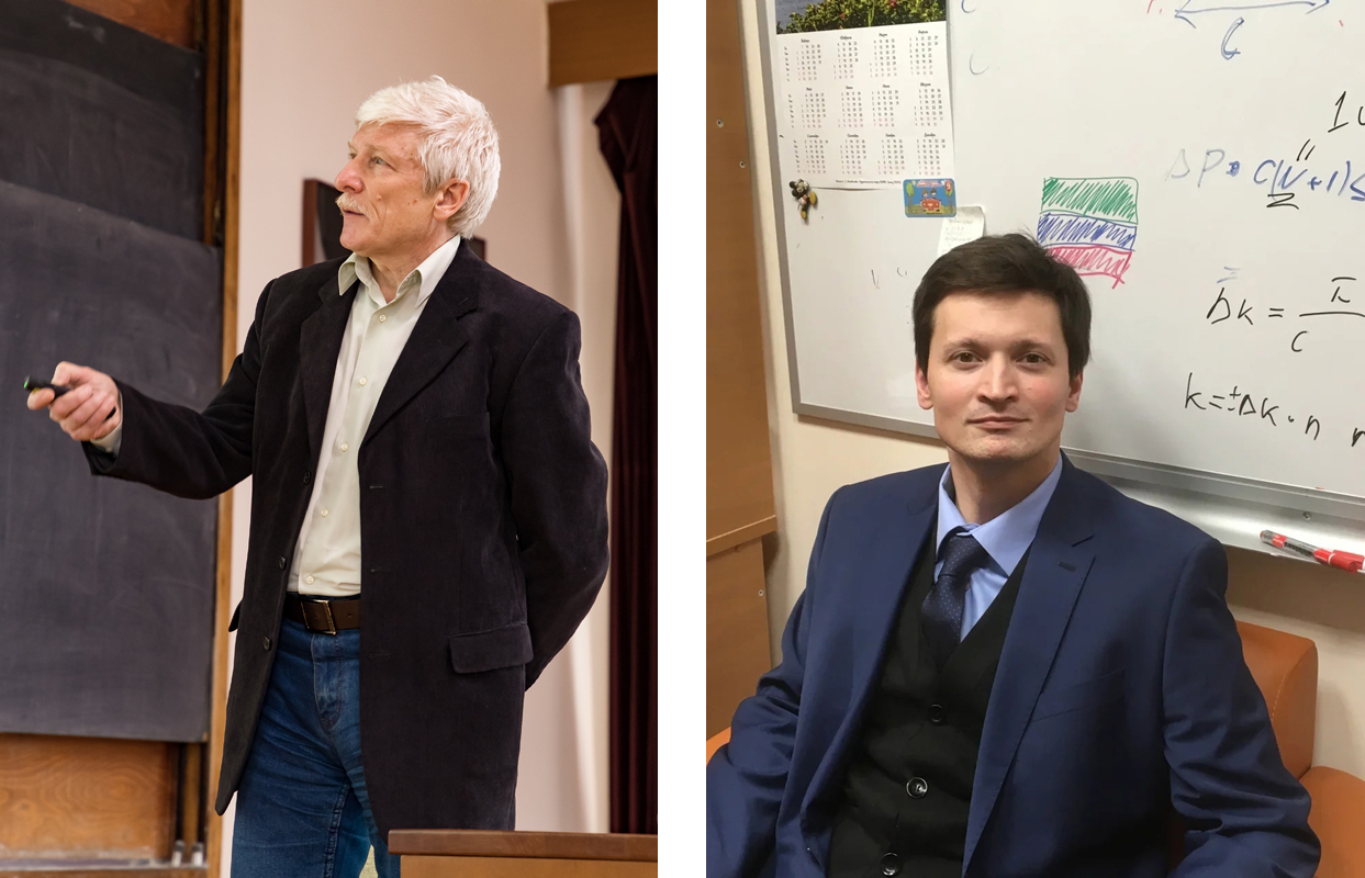 V. A. Osipov (on the left) and V. L. katkov (on the right)
At this stage, the development of electronics has reached a limit, which is primarily due to the properties of the material basis of microelectronic devices, that is, due to the properties of standard semiconductors. In this regard, there is a request to fundamental science regarding the further development of the base for computing technology. One of the answers is the proposal of the fundamentally new materials with unique properties and the development of the ways to use of them to create new, efficient microelectronic devices.
Graphene is one of the main candidates for the role of a basic material for a new type of electronics. The discovery of this two-dimensional material, which is a monolayer of carbon atoms, was awarded the Nobel Prize in physics in 2010. Graphene has a number of advantages over standard semiconductors. The most important is the extremely high mobility of charge carriers (this characteristic is directly responsible for the speed of electronic devices). In addition, the very fact that graphene is two-dimensional (2D) creates the possibility for a compact layout (miniaturization). However, this material also has some disadvantages. If we omit the technological aspects, then they should include the absence of a band gap and the inability to localize electrons in graphene due to the Klein paradox. The development of fundamental principles for the operation of electronic devices, which, on the one hand, use the advantages of graphene, and on the other hand, allow avoiding the difficulties associated with its shortcomings, is an extremely urgent and very interesting scientific task. A huge number of both theoretical and experimental works are devoted to the concepts of various devices of graphene electronics. In particular, active research is underway to create switching devices based on the tunneling effect (there are no components between the contacts), with two main types of layout: vertical and planar. The presented cycle is devoted to devices with a flat (planar) layout. The entire set of modern theoretical approaches used for calculating electron transport was used: the nonequilibrium Green’s function (NEGF) method, recursive NEGF, the Bardeen tunneling Hamiltonian method, as well as the master equation method for calculating the effects associated with the Coulomb blockade. As a result, the authors of the cycle obtained several important theoretical results that clarify the possibility of creating and operating devices for planar tunneling electronics based on graphene:
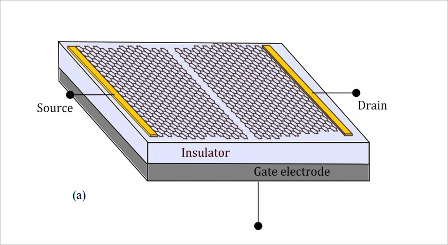
(1) a graphene-based tunneling field-effect transistor operating on new, original principles is proposed. The key factor for its operation is the use of localized electronic states, which are present in graphene at the zigzag edge [3,8,9]. The analysis of the influence of edge defectiveness on the functionality of this device has been carried out [4, 5]. The implantation of vacancies instead of edge atoms is considered as a model of defectiveness. The study showed that localized edge states are very resistant to edge imperfection, which ensures the stable operation of the device up to thirty percent substitution of vacancies for atoms. The proposed switching mechanism fundamentally expands the range of currently known switching electronic devices (transistors). It effectively involves the unique properties of graphene, such as edge states and two-dimensionality, while simultaneously avoiding the influence of the negative factor in the form of the Klein paradox by using the gap between the electrodes (“nanoslits”). The most important characteristic of the efficiency of a transistor is the ON/OFF ratio, which can reach 1000, which is a good indicator for such devices. For this tunneling field-effect transistor, a patent was issued [6].
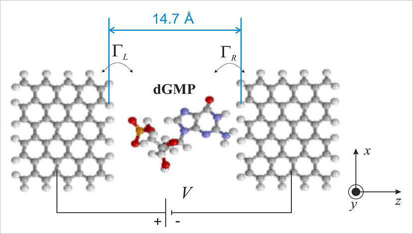
(2) The mechanism of DNA decoding using graphene electrodes separated by a nanogap was investigated [7, 10]. The very principle of the device and the decryption mechanism were proposed earlier by other authors. The main idea here is to use the value of the tunneling current in the graphene/nucleotide/graphene system as a factor for determining the type of nucleotide. Our contribution to the study of this mechanism lies in the fact that we took into account such phenomena as (a) the possibility of random orientation and localization of the nucleotide during its dragging through the nanogap, and (b) the effect of the Coulomb blockade on the tunneling current in this system. As a result of the study, it turned out that both factors noticeably modify the tunneling current in the system, which makes the possibility of decoding nucleotides only by this parameter fundamentally unrealizable in practice. We proposed a way out of this situation: it turned out that if, when carrying out a statistical analysis, not only the average value of the tunneling current, but also its mean-square deviation is used as a factor for nucleotide identification, then the decoding process becomes possible.
(3) An auxiliary part of previous studies is the calculation of tunnel hopping integrals as a function of the distance between atoms. In a situation where the interaction between atoms takes place inside a solid, all such parameters are already well studied and presented in the form of reference tables. At the same time, the tunneling interaction has not yet been described in a similar way, and when calculating the tunneling for the hopping parameters, one or another estimate was used. For current and future research, tunneling hopping parameters were calculated for carbon and a number of chemical elements that make up promising two-dimensional materials. For this, Bardeen’s approach was applied. Atomic orbitals were calculated using the Hartree-Fock method in the framework of the algorithm proposed by Herman and Skillman (Herman, F., Skillman, S .: Atomic Structure Calculations. Prentice Hall, Upper Saddle River (1963)) using Slatter’s X-alpha method. These parameters can be used to solve a wide range of tunneling problems within the framework of the method of linear combination of atomic orbitals [2].
(4) An important way of changing the properties of graphene is associated with its functionalization with various elements and compounds. One of the popular materials obtained in this way is partially fluorinated graphene. One of its advantages is stability and lack of degradation in air, so it can also be considered as a material for planar electronics. Thus, it is extremely important to know the regularities of electron transport at different degrees of fluorination and different methods of fluorine distribution over the graphene surface. Previous experimental studies have shown the presence of a number of features of electron transport in fluorinated graphene, namely, an increase in conductivity upon 10% fluorination and the presence of electron-hole asymmetry. We managed to explain theoretically both of these phenomena [1]. The calculation of such characteristics as the length of electron localization and characteristic temperature, which appears as a parameter in the thermoactivation law of conductivity for different fluorine concentrations and different energies, was performed. To involve real fluorine distributions in the model, a mechanism for the rapid generation of fluorinated structures was proposed , it allows taking into account the fact that in reality fluorine is not uniformly distributed, but forms chains and islands of various sizese. Calculations of the conductivity showed that taking this factor into account is necessary for the model to describe the experimental data. It was found that the electron-hole asymmetry of the characteristic temperature is explained by the asymmetry of the density of states, since the localization length on the energy scale is symmetric over a wide range of fluorine concentrations. The feature of conductivity at 10% fluorine concentration was reproduced in the calculation and turned out to be associated with a resonant increase in the localization length. Fourier analysis of the electron density distribution has illustrated that it is at a ten percent concentration that quasi-periodic electronic domains are formed, which increases the tendency to delocalize the electron and leads to a peak in conductivity. Thus, we were able to explain the experimental behavior of conductivity in fluorinated graphene, to reveal the role of fluorine ordering, and also to predict this behavior for a wide range of concentration (1-20 percent) and energy (-1.5 – 1.5 electron volts).
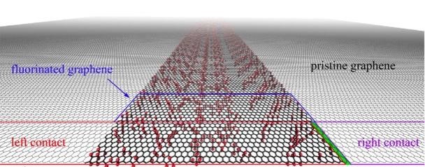
- Effect of fluorine patterns on electronic transport in fluorinated graphene R. D. Yamaletdinov, V. L. Katkov, Y. A. Nikiforov, A. V. Okotrub and V. A. Osipov Advanced Theory and Simulations 3, 1900199 (2020)
- Hopping parameters for tunnel coupling in 2D materials V. L. Katkov, D. A. Lobanov Journal of Computational Electronics 18, 138-145 (2019)
- Review Article: Tunneling-based graphene electronics: Methods and examples V. L. Katkov, V. A. Osipov Journal of Vacuum Science & Technology B 11 (2017)
- Effect of edge vacancies on performance of planar graphene tunnel field-effect transistor A. A. Glebov, V. L. Katkov, V. A. Osipov EPL (Europhysics Letters) 118, 27003 (2017)
- Effect of edge vacancies on localized states in a semi-infinite zigzag graphene sheet A. A. Glebov, V. L. Katkov, V. A. Osipov JETP letters 104, 842-846 (2016)
- Graphene-based tunneling field-effect transistor (Patent No.2554694) by V. L. Katkov, V. A. Osipov, official bulletin “Inventions. Useful models”, 18, 2 554 694 (2015)
- DNA sequencing through graphene nanogap: a model of sequential electron transport O. G. Isaeva, V. L. Katkov, V. A. Osipov The European Physical Journal B 87, 272 (2014)
- Planar graphene tunnel field-effect transistor VL Katkov, VA Osipov Applied Physics Letters 104, 053102 (2014)
- Graphene-based tunnel junction V. L. Katkov, V. A. Osipov JETP letters 98, 689-694 (2014)
- Resonant Tunneling In Graphene-DNA Base-Graphene Junctions V. L. Katkov, O. G. Isaeva, V. A. Osipov Journal of Physics: Conference Series 393, 012026 (2012)
V. L. Katkov (senior researcher, BLTP JINR),
V. A. Osipov (Head of department ‘Condensed matter theory’, BLTP JINR)